Products
Applications
- 5G Products
- Data com
- Server
- Telecom

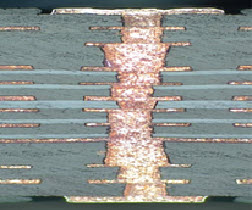
Main PCB Tech.
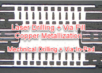
- HDI Process
- Blind / Buried Vias (Mechanical & Laser Drilling)
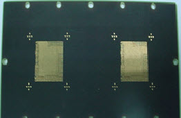
- Embedded Copper Coins
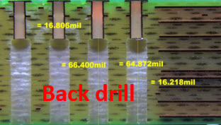
- Back drill
- Via-In-Pad (Resin Or Copper Paste Filled)
Capability
- Layer count: 6~40L
- Board material: Ro4350B、Ro4003C、M6 series 、M7 series、EMC528(HF)、EMC891~K、EMC890~890K(HF)、Isola I-Tera、Isola TerraGreen、Tuc-933、Tuc-883
- Board thickness: 0.18mm min.
- Size: 18" X 23" (Shipping size)
- BGA Pitch: 0.35mm (min)
- Min trace width/spacing: 0.003"/0.003"
- Min thru hole size: 6mils (VIP resin filled) 8mils (VIP copper paste plugged)
- Min gap from PTH to track inner layers: > 6mils
- Thru hole aspect ratio(The board thickness vs.Drill hole size): 8~30
- Min/Max Laser drill hole size: 3mils / 8mils ( VIP plated shut)
- Aspect ratio (dielectric thickness/ Laser drill hole size): 0.8Max.
- HDI: 9+N+9 (Anylayer)
- Back drill: Min hole size 15.7mils Depth tolerance +/-6mils
- Copper coin: length x width 3mm x 3mm(min) Surface flatness:30um(max)
- Layer to Layer Registration: +/-1.5mils min.
- Tolerance of impedance control: +/-5%
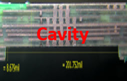
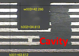
- Cavity Process: By LPKF laser cutting machine
- Board finishings: ENEPIG+Hard gold plating(Gold finger) Soft gold plating+Hard gold plating(Gold finger)
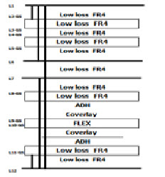
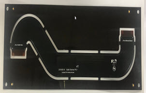
Applications
- High frequency High speed low loss
- High Dk Low loss
- Antenna test board
- Low Noise Block
- VSAT Transceiver
Main PCB Tech.
- HDI
- Blind/buried via (Mechical-drilled)
- Via-In-Pad (Resin Or Copper Paste Filled)
- Cavity Process
Capability
- Layer count: 2~20L
- Board material: Ro3003、Ro3010、RT5870、RT5880、RT6010、Ro4360、TMM10、TMM10i、TACONIC RF series、TACONIC TLY series、High frequency adhesive
- Double-sided process: RT5870、RT5880、RT6010、Ro4360、TMM10、TMM10i
- Hybrid: Ro3003、Ro3010、Ro4360、TACONIC RF series、TACONIC TLY series+ FR4
- Board thickness: 0.18mm(min)
- Size: 0.5" X 0.5" (min)(Shipping size)
- Min trace width/spacing: 0.005"/0.005"
- Tolerance of trace width / spacing: +/-8% trace width > 10mils and tolerance: +/-1mils
- Radius of Antenna width: 0.5mils(max)
- Min gap from Antenna to conductors: 3mils(min)
- Min thru hole size: 6mils (VIP resin filled) 8mils (VIP copper paste plugged)
- Min gap from hole edge to hole edge (Stitching via): 8mils
- Min gap from hole edge to copper (Stitching via): 6mils
- Aspect ratio: dielectric thickness / Laser drill hole size: 5mils / 6.50 mils(max) ( VIP plated shut )
- HDI: 1+N+1
- Layer to Layer Registration: +/-1.50 mils
- Tolerance of impedance contro: +/-5%
- Cavity Process: Lamination (Adhesive Low Dk Low Df)+depth control milling、LPKF depth control mill down
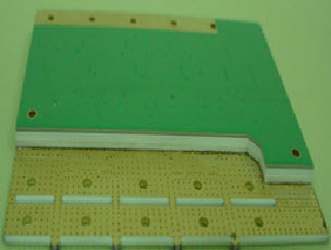
Applications
- High performance heat dissipation metal core
- LED
- Work Station Power Supply
- Base Station Transceiver
Main PCB Tech.
- Standard PCB process
- Cavity Process
Capability
- Layer count:
-
- Single-sided single layer MCPCB (Aluminum core or Copper Plates)
- Single-sided multi-layer MCPCB (Aluminum core or Copper Plates)
- Double-sided single layer MCPCB (Metal Core interlay) (Aluminum core or Copper Plates)
-
Board material:
- Thermal conductivity: Ventec VT-4A VT-4B
- Thickness: 2~6mils Thermal conductivity:2.2~7 (W/m*k)
- Aluminum core: 5XXX、6XXX
- Thickness: 0.8mm~3mm
- Copper Plates
- Thickness: 0.8mm~3mm
- Chip on Metal:
-
- Cavity Process: Lamination (nonflow Prepreg)+depth control milling、LPKF depth control mill down
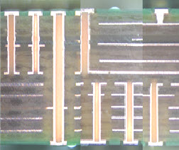
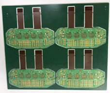
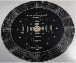
Applications
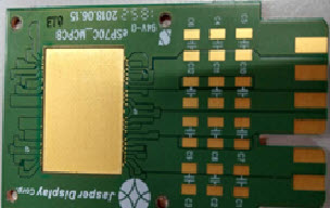
- Load Board
- Probe Card
Main PCB Tech.
- HDI Process
- Blind / Buried Vias (Mechanical & Laser Drilling)
- Back drill
- Via-In-Pad (Resin Or Copper Paste Filled)
Capability
- Layer count: 10~50L
- Board material: FR4 FR4-HTG or others
- Board thickness: 2mm~6.3mm
- Size: 18" X 23" (Shipping size)
- BGA Pitch: 0.35mm (min)
- Min trace width/spacing: 0.003" / 0.003"
- Min thru hole size: 6mils (VIP resin filled) 8mils (VIP copper paste plugged)
- Min gap from PTH to track inner layers: > 5mils
- Thru hole aspect ratio (The board thickness vs.Drill hole size): 8~30
- Min/Max Laser drill hole size: 3mils / 8mils (VIP plated shut)
- Aspect ratio (dielectric thickness / Laser drill hole size): 0.8Max.
- HDI: 9+N+9 (Anylayer)
- Back drill: Min hole size 15.7mils Depth tolerance +/-6mils
- Layer to Layer Registration: +/-3mils
- Tolerance of impedance control: +/-5%
- Warpage (Load Board / Probe Card): 4mil/inch / 1mils/inch
- Board finishings: Hard/Soft gold, ENIG
- Contersink: Y (θ: 82 degree, 90 degree & 100 degree)
- Conterbore: Y
Applications
- Jedec/droptest/burn in
- Interposer
Main PCB Tech.
- HDI
- Blind/buried via (Mechical-drilled)
- Via-In-Pad (Resin Or Copper Paste Filled)
Capability
- Jedec/drop test/burn in
-
- Layer count: 2~14L
- Board material: FR4 FR4-HTG Polyimide (ARLON 85N、Ventec VT-90H) or others
- Board thickness: 0.9~2.0mm
- Size: 18" x 23" (Shipping size)
- Min thru hole size: 6mils (VIP resin filled)
- Min gap from PTH to track inner layers: > 5mils
- BGA Pad Size: 10mils(min) for Thru hole 6mils(min) for Laser-drilled
- Tolerance of BGA Pad size: +/-10%
- Gap between BGA PAD and solder mask opening: 1.2mils(min)
- Gap for BGA solder dam clearance:3mils(min)
- Layer to Layer Registration: +/-3mils
- Min/Max Laser drill hole size: 3mils / 8mils (VIP plated shut)
- Aspect ratio (dielectric thickness / Laser drill hole size): 0.8Max.
- Interposer
-
- Layer count: 2~14LL
- Board material: FR4 FR4-HTG Adhesive Polyimide
- Board thickness: 2.0~5.0mm
- Size: 6" x 6"(max) (Shipping size)
- BGA Pad pitch-0.15mm
- Min. BGA Pad size/spacing: 4/2mils
- Min Laser via size/deilectric thickness: 2/1.5mils
- Board finishing: ENIG
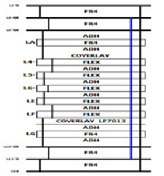
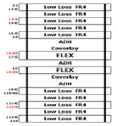
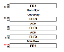
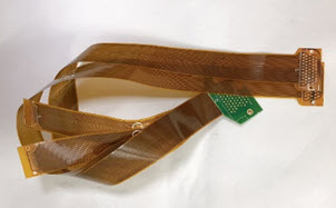
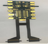
Applications
- Flex
- Rigid-flex board
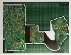
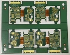
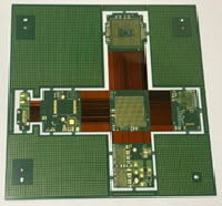
Main PCB Tech.
- HDI Process
- Blind / Buried Vias (Mechanical & Laser Drilling)
- Via-In-Pad (Resin Or Copper Paste Filled)
- Cavity Process
- Board finishings: Optional
Capability