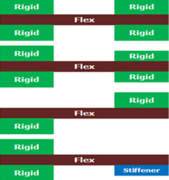
Rigid-Flex
Stack up TYPE
| Description | Production | Advanced |
|---|---|---|
Rigid + FLEX (Air Gap) + Rigid
|
Yes | Yes |
FLEX+ rigid

|
Yes | Yes |
Board Dimensions
| Description | Production | Advanced |
|---|---|---|
| Max. Finish Board Size | 16」X20」 | 18」X26」 |
| min. Finish Board Size | 0.2"x0.2" | 0.15"*0.15" |
| Max. Board Thickness | 0.250"(+/-10%) | 0.280"(+/-8%) |
| Min. Board Thickness | 0.016"(+/-10%) For 4L | 0.016"(+/-10%) For 4L |
Lamination
| Description | Production | Advanced |
|---|---|---|
| Layer Count | 4~42L | 50L |
| Layer to Layer Registration | +/-4mils | +/-2mils |
Drilling
| Description | Production | Advanced |
|---|---|---|
| Min. Drill Size | 6mils | 5mils |
| Min. Hole to Hole Pitch | 16mils(0.5mm) | 18mils(0.35mm) |
| True position Tolerance | +/-3mils | +/-2mils |
| Slot Diameter Tolerance | +/-3mils | +/-2mils |
| Min gap from PTH to track inner layers | 5mils | 4mils |
| Min gap from PTH to the border of rigid flex | 30mils | 20mils |
| Min. PTH Hole edge to PTH Hole edge space | 8mils | 6mils |
Plating
| Description | Production | Advanced |
|---|---|---|
| Max. Aspect Ratio | 8:1 | 10:1 |
| Cu Thickness in Through hole | >1mils | >1mils |
| Plated hole size tolerance | +/-2mils | +/-1.5mils |
| NPTH hole tolerance | +/-2mils | +/-1mils |
| Via in pad Fill Material | Epoxy resin/Copper paste | Epoxy resin/Copper paste |
Layer
| Description | Production | Advanced |
|---|---|---|
| Min. Trace/Space | 2.5mils / 2.5mils | 2mils / 2mils |
| Min. pad over drill size | 6mils | 4mils |
| Max. Copper thickness | 1~2 oz | 3 oz |
| Line/ pad to board edge | 6mils | 4mils |
| Min gap from Copper to the border of rigid flex | 10mils | 8mils |
| Line Tolerance | +/-15% | +/-10% |
Metal Finish
| Description | Production | Advanced |
|---|---|---|
| HASL | 50-1000u」 | 50-1000u」 |
| HASL+Selective Hard gold | Yes | Yes |
| OSP | 8-20u」 | 8-20u」 |
| Selective ENIG+OSP | Yes | Yes |
| ENIG(Nickel/Gold) | 80-200u」/2-9 u」 | 250u」/ 10u」 |
| Immersion Silver | 6-18u」 | 6-18u」 |
| Hard Gold for Tab | 10-80u」 | 10-80u」 |
| Immersion Tin | 30u」min. | 30u」 min. |
| ENEPIG (Ni/Pd/Au) | 125u"/4u"/1u」 min. | 150u"/8u"/2u」 min. |
| Soft Gold (Nickel/ Gold) | 200u」/ 20u」min. | 200u」/ 20u」 |
Coverlay
| Description | Production | Advanced |
|---|---|---|
| Thickness(Min) (PI / ADH) | 0.5mils / 1mils | 0.5mils / 1mils |
| dam width | 20mils | 15mils |
| registration tolerance | +/-10mils | +/-8mils |
Solder Mask
| Description | Production | Advanced |
|---|---|---|
| S/M Thickness | 0.4mils min. | 3mils max. |
| Solder dam width | 4mils | 3mils |
| S/M registration tolerance | +/-2.5mils | +/-2mils |
| S/M over line | 3.5mils | 2mils |
Legend
| Description | Production | Advanced |
|---|---|---|
| Min. Space to SMD pad | 6mils | 4mils |
| Min. Stroke Width | 6mils | 5mils |
| Min. Space to Copper pad | 6mils | 4mils |
| Standard Color | White or Yellow | N/A |
Electrical Testing
| Description | Production | Advanced |
|---|---|---|
| Max. Test Points | 30000 Points | 30000 Points |
| Smallest SMT Pitch | 20mils | 16mils |
| Smallest BGA Pitch | 20mils | 16mils |
laser Rout (LPKF)
| Description | Production | Advanced |
|---|---|---|
| Min. Rout to copper space | 6mils | 4mils |
| Rout tolerance | +/-2mils | +/-2mils |
NC Rout
| Description | Production | Advanced |
|---|---|---|
| Min. Rout to copper space | 8mils | 4mils |
| Rout tolerance | +/-4mils | +/-3mils |
Impedance controll
| Description | Production | Advanced |
|---|---|---|
| Impedance controll | +/-8% | +/-5% |
EMI
| Description | Production | Advanced |
|---|---|---|
| PC-5500&PC-5600 | Yes | Yes |
Stiffener
| Description | Production | Advanced |
|---|---|---|
| PI | Yes | Yes |
| FR4 | Yes | Yes |
| Metal | Yes | Yes |
Conductive & thermal adhesive
| Description | Production | Advanced |
|---|---|---|
| 3M Type | Yes | Yes |
Eccobond
| Description | Production | Advanced |
|---|---|---|
| Eccobond over Flex width | 60mils | 60mils |